- 您现在的位置:买卖IC网 > Sheet目录479 > MMFT5P03HDT1 (ON Semiconductor)MOSFET P-CH 30V 3.7A SOT223
�� �
�
�MMFT5P03HD�
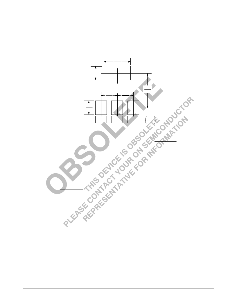
�INFORMATION� FOR� USING� THE� SOT� ?� 223� SURFACE� MOUNT� PACKAGE�
�MINIMUM� RECOMMENDED� FOOTPRINT� FOR� SURFACE� MOUNTED� APPLICATIONS�
�Surface� mount� board� layout� is� a� critical� portion� of� the�
�total� design.� The� footprint� for� the� semiconductor� packages�
�must� be� the� correct� size� to� insure� proper� solder� connection�
�interface� between� the� board� and� the� package.� With� the�
�correct� pad� geometry,� the� packages� will� self� align� when�
�subjected� to� a� solder� reflow� process.�
�0.15�
�3.8�
�0.079�
�2.0�
�0.248�
�0.079�
�2.0�
�0.091�
�2.3�
�0.091�
�2.3�
�6.3�
�0.059�
�1.5�
�0.059�
�1.5�
�0.059�
�1.5�
�inches�
�mm�
�SOT� ?� 223� POWER� DISSIPATION�
�T� J(max)� ?� T� A�
�R� θ� JA�
�The� power� dissipation� of� the� SOT� ?� 223� is� a� function� of�
�the� drain� pad� size.� This� can� vary� from� the� minimum� pad�
�size� for� soldering� to� a� pad� size� given� for� maximum� power�
�dissipation.� Power� dissipation� for� a� surface� mount� device� is�
�determined� by� T� J(max)� ,� the� maximum� rated� junction�
�temperature� of� the� die,� R� θ� JA� ,� the� thermal� resistance� from�
�the� device� junction� to� ambient,� and� the� operating�
�temperature,� T� A� .� Using� the� values� provided� on� the� data�
�sheet� for� the� SOT� ?� 223� package,� P� D� can� be� calculated� as�
�follows:�
�P� D� =�
�The� values� for� the� equation� are� found� in� the� maximum�
�ratings� table� on� the� data� sheet.� Substituting� these� values�
�into� the� equation� for� an� ambient� temperature� T� A� of� 25� °� C,�
�one� can� calculate� the� power� dissipation� of� the� device� which�
�in� this� case� is� 3.13� watts.�
�P� D� =� 150� °� C� ?� 25� °� C� =� 3.13� watts�
�40� °� C/W�
�The� 40� °� C/W� for� the� SOT� ?� 223� package� assumes� the� use�
�of� the� recommended� footprint� on� a� glass� epoxy� printed�
�circuit� board� to� achieve� a� power� dissipation� of� 3.13� watts.�
�There� are� other� alternatives� to� achieving� higher� power�
�dissipation� from� the� SOT� ?� 223� package.� One� is� to� increase�
�the� area� of� the� drain� pad.� By� increasing� the� area� of� the� drain�
�pad,� the� power� dissipation� can� be� increased.� Although� one�
�can� almost� double� the� power� dissipation� with� this� method,�
�one� will� be� giving� up� area� on� the� printed� circuit� board�
�which� can� defeat� the� purpose� of� using� surface� mount�
�technology.�
�Another� alternative� would� be� to� use� a� ceramic� substrate�
�or� an� aluminum� core� board� such� as� Thermal� Clad� t� .� Using�
�a� board� material� such� as� Thermal� Clad,� an� aluminum� core�
�board,� the� power� dissipation� can� be� doubled� using� the� same�
�footprint.�
�http://onsemi.com�
�9�
�发布紧急采购,3分钟左右您将得到回复。
相关PDF资料
MMFT960T1
MOSFET N-CH 60V 300MA SOT223
MMG3002NT1
IC AMP RF GP 3600MHZ 5.2V SOT-89
MMG3006NT1
TRANS GPA 33DBM 16-QFN
MMG3007NT1
IC AMP RF GP 6000MHZ 5V SOT-89
MMG3H21NT1
TRANS HBT 20.5DBM 19.3DB SOT-89
MMH3111NT1
TRANS GAAS HFET SOT-89
MML20211HT1
IC LNA 2GHZ 21P1DB 8DFN
MMS-1A-V2 0
SENSOR MICRO MACHINED SMD
相关代理商/技术参数
MMFT5P03HDT3
制造商:MOTOROLA 制造商全称:Motorola, Inc 功能描述:TMOS P-CHANNEL FIELD FEECT TRANSISTOR
MMFT6N03HD
制造商:MOTOROLA 制造商全称:Motorola, Inc 功能描述:TMOS POWER 6.0 AMPERES 30 VOLTS
MMFT960T1
功能描述:MOSFET 60V 300mA N-Channel RoHS:否 制造商:STMicroelectronics 晶体管极性:N-Channel 汲极/源极击穿电压:650 V 闸/源击穿电压:25 V 漏极连续电流:130 A 电阻汲极/源极 RDS(导通):0.014 Ohms 配置:Single 最大工作温度: 安装风格:Through Hole 封装 / 箱体:Max247 封装:Tube
MMFT960T1_06
制造商:ONSEMI 制造商全称:ON Semiconductor 功能描述:Power MOSFET 300 mA, 60 Volts N−Channel SOT−223
MMFT960T1G
功能描述:MOSFET 60V 300mA N-Channel RoHS:否 制造商:STMicroelectronics 晶体管极性:N-Channel 汲极/源极击穿电压:650 V 闸/源击穿电压:25 V 漏极连续电流:130 A 电阻汲极/源极 RDS(导通):0.014 Ohms 配置:Single 最大工作温度: 安装风格:Through Hole 封装 / 箱体:Max247 封装:Tube
MMFTN123
制造商:Diotec Semiconductor 功能描述:
MMFTN138
制造商:Diotec 功能描述:Bulk
MMFTN170
制造商:Diotec Semiconductor 功能描述: